Low-Energy Electron Diffraction – LEED
Spot Profile Analysis – SPA-LEED
A workhorse of the surface physics world is LEED. Low energy electrons of a collimated beam, made to impinge on a sample will be back-scattered from the surface in characteristic ways indicative of the sample structure. The diffracted beams are displayed on a phosphor screen as spots, and they appear in a sharp, periodic pattern for atomically clean crystalline samples like I use. If the order of the sample surface is perturbed, by addition of a layer of something else on top or removal of some surface atoms by sputtering, the pattern changes. SPA-LEED quantifies these changes in order to understand how the perturbation has changed the surface. I have written a robust image analysis suite to analyze images of LEED patterns, and I now use this to analyze progressions of LEED images taken after increments of sputtering to understand how the surface structure changes.
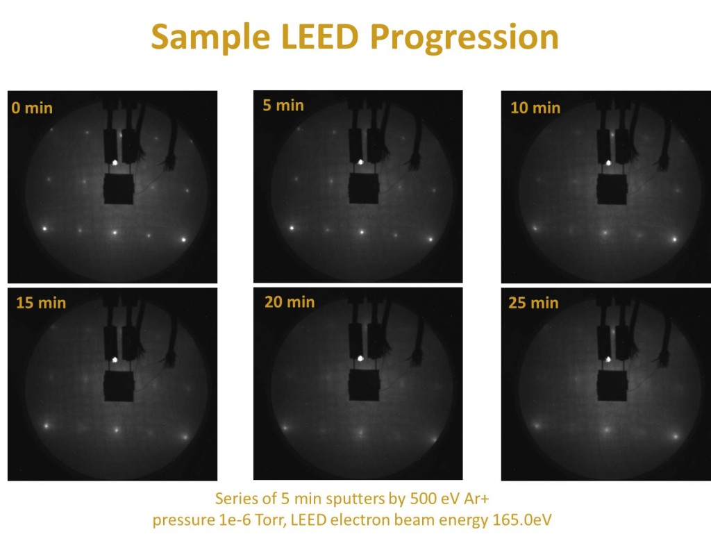
An example is shown below. Each image in the set is the LEED pattern observed for a single crystal Ni(110) sample, which is hanging in the foreground. At top left is the atomically clean surface at 0 min. sputtering dose, showing clean, tight diffraction beams (which appear as spots) against the background. For the 5, 10, etc. minute doses of sputtering damage, we see the beams broaden and reduce in intensity relative to the background.

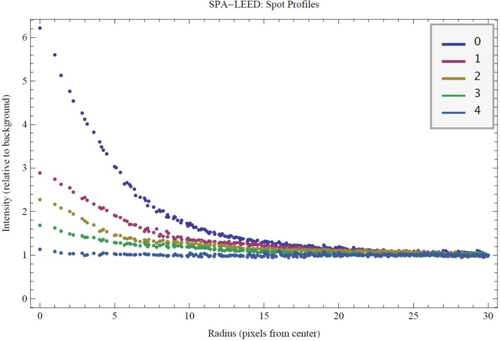
I can pick any of the diffraction spots in a sequence of images and analyze the progression with my SPA-LEED software to produce a map of the damage as indicated by that spot. The image below is one result. For the selected dot in each of the images in a sequence, the trace displays intensity vs. distance from the spot center. Subsequent traces represent the modification for an additional 5 minutes of sputter dose by 500 eV Ar+ ions (blue 0 = clean, purple 1 = 5 min. dose, gold 2 = 10 min. dose, and so on). The integrated area above the background represents the total spot intensity at each increment of sputtering.
